


Silicon Carbide (SiC): Next-generation power electronics
SiC MOSFETs could replace Si IGBTs for high-voltage applications.

In 2018, Tesla became the first EV manufacturer to adopt ST Microelectronics' silicon carbide-based inverter for the Model 3. It allowed them to offer higher power densities, thermal performance at half the size of a traditional power control unit (PCU).
Background
Traditionally, silicon (Si) power electronics are often employed in high-power applications, such as electric drive systems.
However, silicon-based semiconductors have inherent limitations, such as high switching losses, and limited switching speeds.
Switching devices
The two most popular power switching devices are the IGBT (insulated-gate bipolar transistor) and MOSFET (metal oxide semiconductor field-effect transistor).
Traditionally, silicon-based MOSFETs are used for low voltage, lower power and high frequency applications. They dominate the market for applications below 600 volts.
Silicon-based IGBTs are used for high voltage, higher power and low frequency applications. They dominate the market for applications between 600 volts and 6.5kV.
Most EV inverters before the Model 3 used IGBT transistors.
However, with the advent of the EV and modern power electronics, manufacturers are pushing for more efficiency, and lower operating costs. Due to a (relative) lack of efficiency of Si-based power electronics, you need active or large passive cooling systems, which are heavy and expensive.
This is where SiC (silicon carbide) technology comes in.
Intro to Silicon Carbide
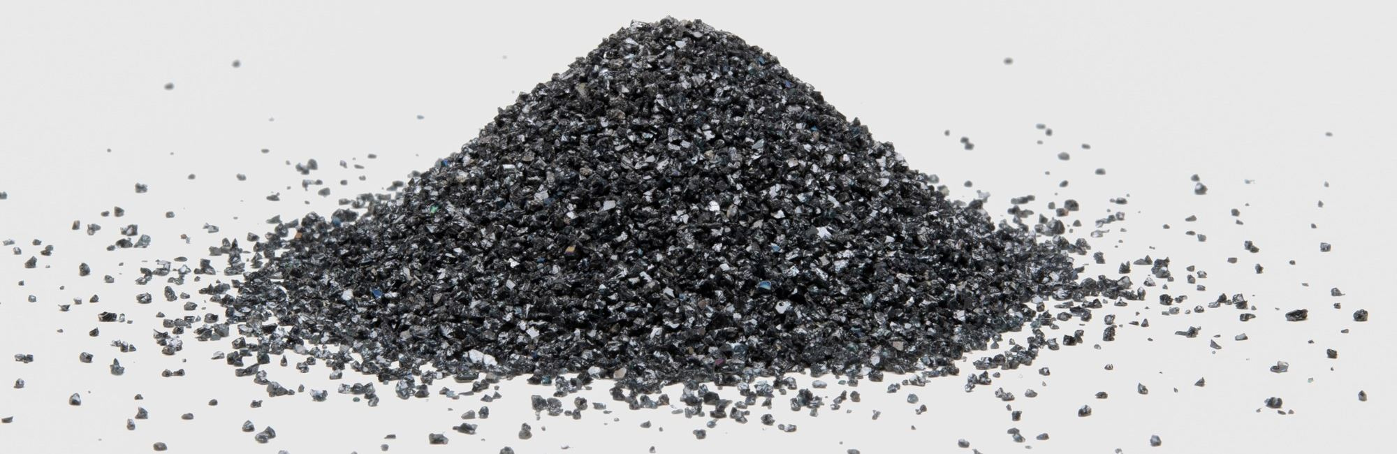
Silicon carbide is a compound material made from silicon and carbon.
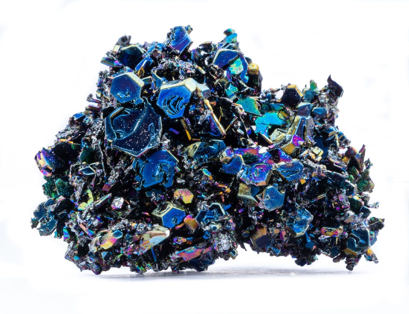
Each silicon atom in the crystal structure is bonded to four carbon atoms, and vice versa, forming a very strong tetrahedral crystal structure. [1]

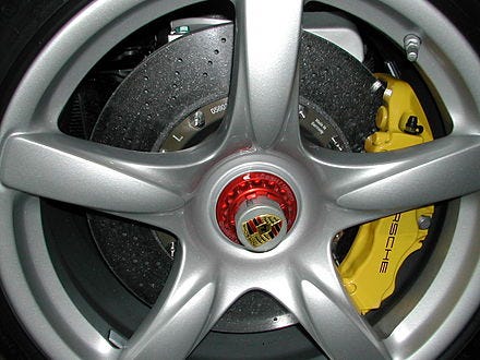
This robust bonding results in exceptional thermal and mechanical properties. That’s why silicon carbide is also widely used in high-stress applications, such as car brakes, car clutches and ceramic plates in bulletproof vests.
The under-appreciated thing is, SiC is also a good semiconductor material. It’s known as a wide bandgap semiconductor.
Wide-bandgap materials
A bandgap is the energy required to “free” an outer shell electron so it can move freely inside a solid.
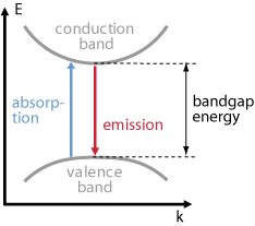
It’s also expressed as the energy difference between the top of the valence band and bottom of the conduction band in semiconductors.
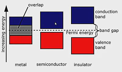
Wide-bandgap semiconductors are semiconductor materials which have a larger bandgap than conventional semiconductors.

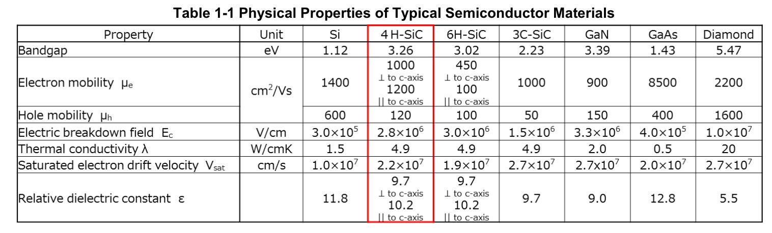
Conventional semiconductors like silicon have a bandgap in the range of 0.6 - 1.5 electronvolts (eV), while wide-bandgap materials typically have bandgaps above 2 eV.
This allows wide-bandgap semiconductors like silicon carbide (SiC) to operate at much higher voltages, frequencies and temperatures than conventional semiconductors like silicon and gallium arsenide.

Specially for silicon carbide (SiC), it has a dielectric breakdown strength of nearly ten times of silicon (Si).
Here’s the thing: the lower the “insulation strength”, the more base material you need to start with. This causes more resistance, is more bulky, but more importantly, it also causes the device to operate slower.

To understand why silicon carbide (SiC) is such a big deal for the future of power electronics, it’s perhaps useful to take a step back and ask ourselves: what makes an ideal switch? (i.e. switching device like the MOSFET or IGBT as mentioned above).
An Ideal Switch

An ideal switch has infinite resistance when it’s “off”. You can block a high voltage, say 1000V, without leaking any current.
An ideal switch has zero resistance when it’s “on”. Zero conduction losses or voltage drop.
(Somewhat less related: An ideal switch will also be able to switch instantaneously, without any lag. You can toggle it back and forth at 100 MHz, and you won’t be constrained by the “rise” and “fall” time.)
Obviously, real-world devices will always have leakage current, some conduction losses / voltage drop, and non-negligible rise times.
How do we get as close as possible to theoretical possibility?
Resistance
Let’s look at a MOSFET. There’s a concept called on-resistance (Rds).
The resistance of the drift region accounts for a large percentage of the on-resistance of high-voltage MOSFETs.

To reduce the on-resistance, you can either increase the dopant concentration, or reduce the drift region thickness.

But the more the dopant concentration, the lower the “withstand voltage”.
Silicon (Si) has low voltage breakdown strength, so it’s impossible to further increase the dopant concentration without compromising the withstand voltage.
It’s also difficult to reduce the thickness of the drift region because the expansion of the depletion region could cause “punch-through” (between drain and source) when a reverse bias is applied across drain and source.

This is where wide-bandgap materials like silicon carbide (SiC) comes in.
SiC dielectric breakdown strength is nearly ten times of silicon. Hence, SiC makes it possible to increase the dopant concentration in the drift region, and thereby reduce it’s thickness to obtain the same withstand voltage. [2]
(Electron and hole mobilities (μ) characterize how quickly an electric field can accelerate the velocity of an electron or a hole (velocity = mobility (μ) × electric field (E)). A higher mobility (μ) means that an electric current flows more easily, resulting in lower resistance. The maximum velocity attainable is called the saturation velocity.)
SiC makes it possible to create high-voltage power devices with unprecedentedly low on-resistance thanks to a heavily doped, thin drift region.

Kreutzer et al. have developed high-efficiency DC/DC converters using SiC MOSFETs at both low power (15 kW with 98% efficiency and high power (100 kW with 99.7% efficiency, with verified voltage capability at high on-board voltage (800 V). SiC on-board DC/DC converters also achieve a high power density of 43 kW/L, the highest reported in previous studies. For the auxiliary power supply in vehicles, in a 400 V to 12 V soft-switching DC/DC converter achieving 87% efficiency is designed.
Kreutzer Otto, A passively cooled 15 kW, 800 V DCDC-converter with a peak efficiency of 99.7 %
If SiC has so many advantages over Si, then why haven’t they been more widely adopted?
Why haven’t we seen SiC-based power electronics in the market until very recently?
Part of the answer is materials science.
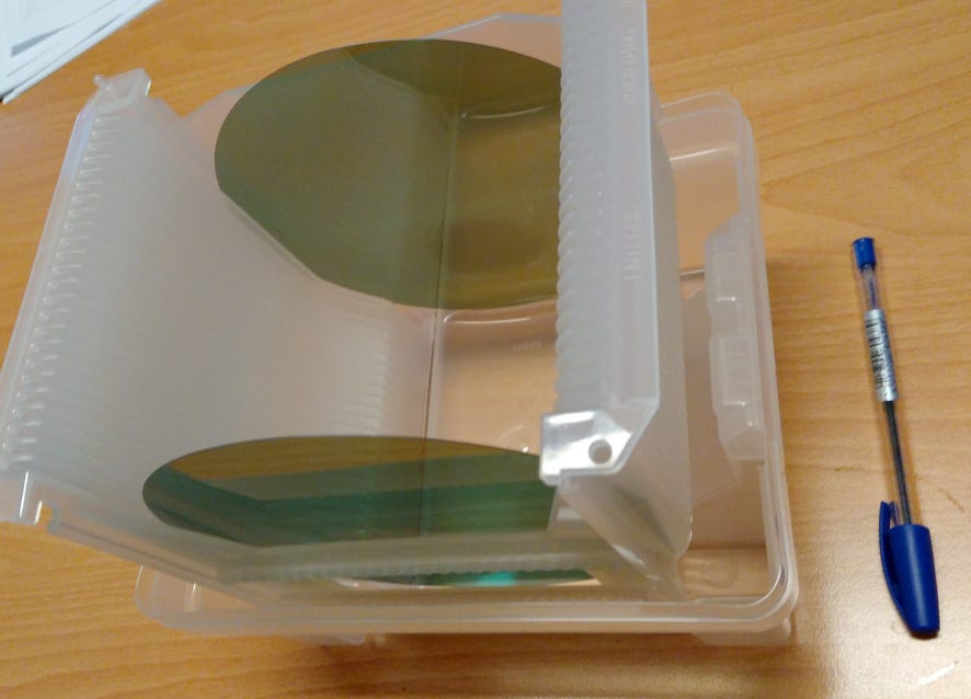
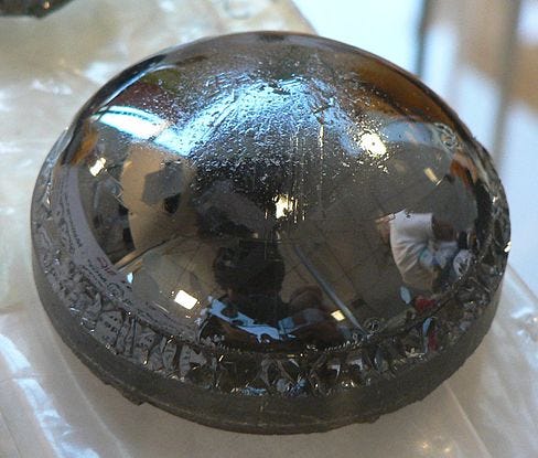
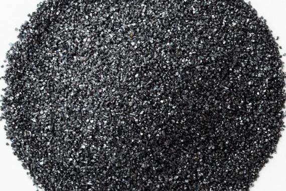
Producing high quality SiC wafers is hard.
One of the major problems for SiC commercialization was the elimination of defects - edge dislocations, screen dislocations, basal plane dislocations etc.
The traditional Czochralski method — which relies on liquid silicon melt — doesn’t work for SiC.
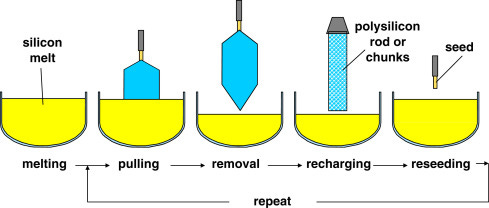
Silicon Carbide solid form directly passes into the gaseous form, without first turning into a liquid. Because of this, there’s no melt and SiC cannot be made with traditional silicon methods. The only way to grow the silicon carbide crystals is from gas.
Until 1950, the only commercial way to make silicon carbide was the Acheson method.
“In the Acheson process, pure silica sand and finely divided carbon (coke) are reacted in an electric furnace at temperatures in the range of 2,200°–2,480° C (4,000°–4,500° F)”

This was useful for making abrasives such as sandpaper. But not the purity requirements for electronics.
In 1954, Jan Anthony Lely discovered the Lely method.
Take a tube of porous graphite and surround it with silicon carbide. then you heat the tube to 2500 Celcius. Silicon carbine will diffuse its way to the inside of the tube, and crystallize on its cooler parts. Lely’s early method created randomly sized, hexagon-shaped platelets of varying crystal polytypes. It was a step forward, but still not suitable for wafers.
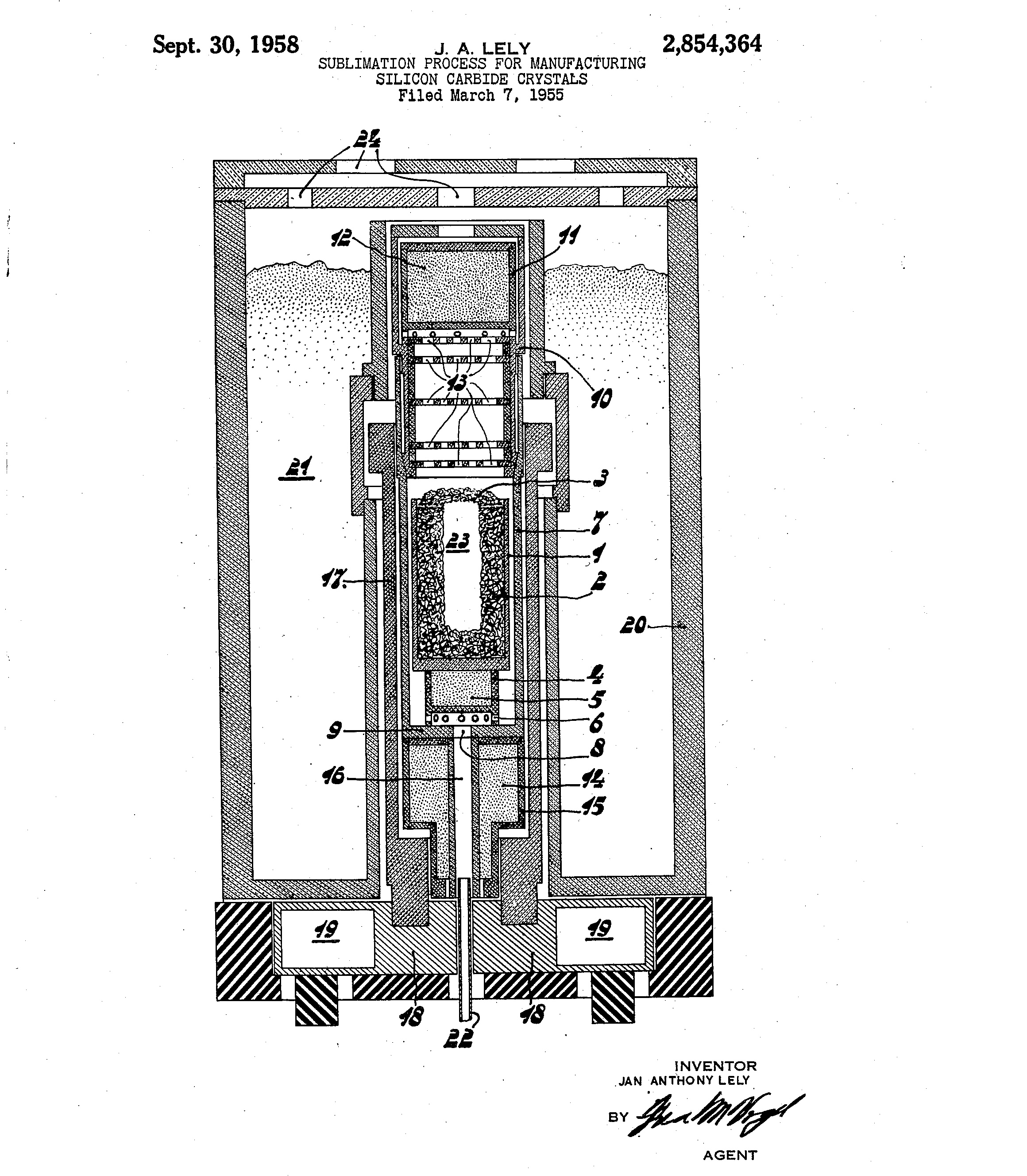
So, in 1978, two Soviet scientists Tairov and Tsvetkov modified the Lely process to fix it’s shortcomings. It works mostly the same way, but with careful control of temperatures and pressures, scientists could grow one large crystal of a single polytype.

This modified Lely method is called physical vapor transportation or PVT.
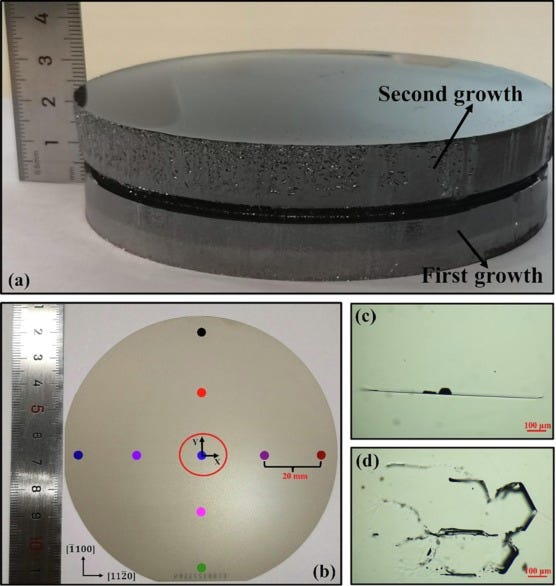
This meant that people can grow boules of one pure Silicon Carbide polytype at a rate of a few millimeters per hour. Still not perfect, but getting better and better.
Difficulties in marking SiCs transistors
SiC wafers can only be cut with synthetic diamonds or lasers. Diffusing dopants also need very high temperatures. The same atomic bonding that makes SiC hard also makes it a pain in the butt to chemically etch.
Acids don’t do anything to it, and basically the only way to etch it is high-power plasma etching. (plasma etching is common, but SiCs need a serious bombardment before any of it goes away)
Hence, for many years, the performance improvements offered by SiC did not sufficiently outweigh the cost advantages outside of high-end applications like aerospace or military. Also suffered from reliability issues due to handling higher thermal conductivity, dealing with different electrical characteristics.
Recent advancements have addressed many of these issues around cost reduction, better supply chain and advancements in device design and packaging.
Commercialization
Infineon introduced the first commercial silicon carbide-based power device in 2001 - scottsky diode.
Commercial SiC MOSFET was first released in 2011 by a North Carolina-based company called Cree (now renamed to Wolfspeed).
Other companies soon jumped in like ST Microelectronics, ROHM, Infineon and Microsemi.

The 1.2 kV class became the entry and dominant point for SiC MOSFETs in the market, as this is the breaking point between Si MOSFETs and Si IGBT.
SiC MOSFET provides excellent balance between conduction loss and switching loss at blocking voltages of less than 2.5 to 3.3 kV.
Cost
There’s still price gap with traditional Si, albeit steadily shrinking.
EV driving alot of demand, and hence learning curves. Cost will continue to drop → A number of automobile manufacturers are already planning to incorporate silicon carbide into power electronic devices in their products.
Wolfspeed also recently opened a large silicon carbide plant in 2022, in upstate New York to ramp up production.
Interestingly enough, even with the price gap, power electronics engineers can design with systems with less balance-of-plant (cooling, additional switches etc.) The space, cost and size savings add up, and I anticipate SiC MOSFETs will start challenging Si IGBTs in traditional market strongholds.
“Beyond the transistor itself, building a power converter requires passive components. Capacitors and inductors. Transistors switch almost a million times per second and passive components act as energy reservoirs to smooth out voltage and/or current. The faster the switching speed, the less time the passives need to plug the gap for, and the smaller they can be. When it comes to capacitors and, particularly, inductors, a larger capacitance/inductance value means a physically larger and heavier component. Fast-switching SiC MOSFETs (they switch much faster than a Si IGBT of the same voltage/current rating) mean smaller, lighter, cheaper passive components, and this is where the bulk of the efficiency saving comes from (although faster switching normally also means lower losses in the conversion itself, so higher efficiency and less heat generated).”
Appendix
Electromagnetic interference (EMI) considerations
“While SiC MOSFETs have the advantage of high switching speeds resulting in low switching losses, high switching speeds also mean rapid changes in voltage and current (high dv∕dt and di∕dt). SiC MOSFETs have approximately 10 times the switching speed of Si-IGBTs Replacing Si-IGBTs with SiC MOSFETs in the same circuit topology will accordingly increase dv∕dt and di∕dt in the circuit in which they are located by a fac- tor of 10. These rapid voltage and current changes can cause inductive and capacitive components in the loop to generate up to 10 times the peak voltage or current [56]. This makes SiC MOSFETs more sensitive to parasitic parameters in the circuit such as stray inductances and capacitances. The higher peak voltages or currents cause more serious electromagnetic interference (EMI) problems [57], which affect the performance of the control loop and the stability of the power system. In addition, the positive and negative transient overvoltages in SiC MOSFET modules can exceed the device’s stress limit due to the effect of parasitics [58], which can damage the device. Furthermore, the higher switching frequency and higher switching speeds make SiC MOSFETs more sensitive when it comes to cable length. Long cables between devices can cause transient overvoltage problems at terminals due to their large parasitic inductances [62], which can lead to a failure of the insulation and resulting leakage currents.”
Power loss comparison with Si IGBT
SiC MOSFETs are starting to replace Si IGBTs. MOSFETs generally operate at lower voltage/current and higher frequency than IGBTs. But SiC beats that tradeoff and allows SiC MOSFETs to match the voltage/current ratings of IGBTs, but with lower switching losses and higher switching frequencies.
These are exciting times to be a power enthusiast.
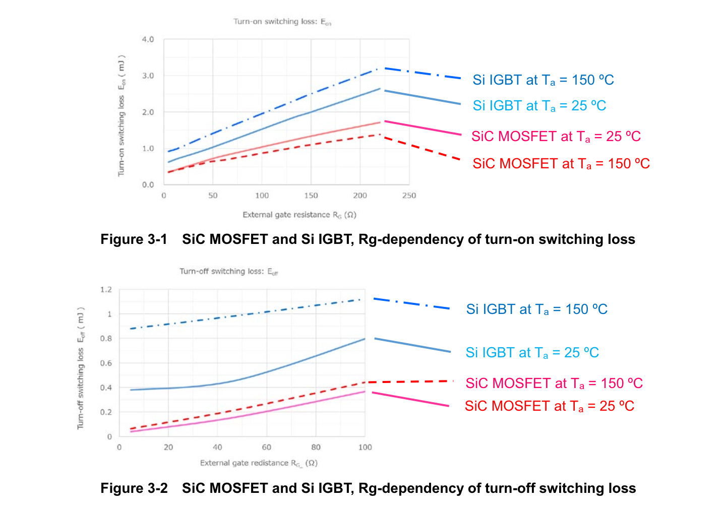
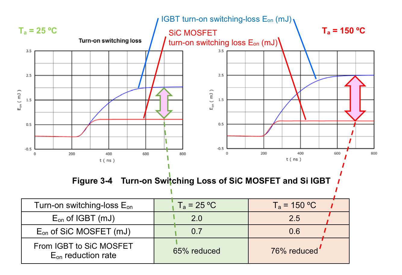

Lower losses = lower heat generation.


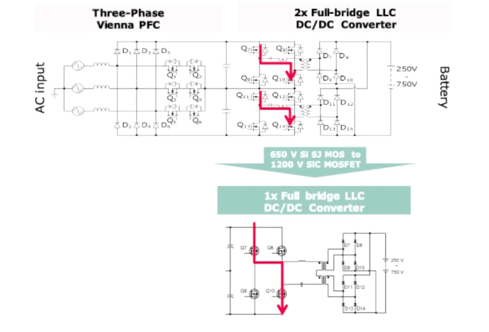
Simplified & reduced part count in topologies
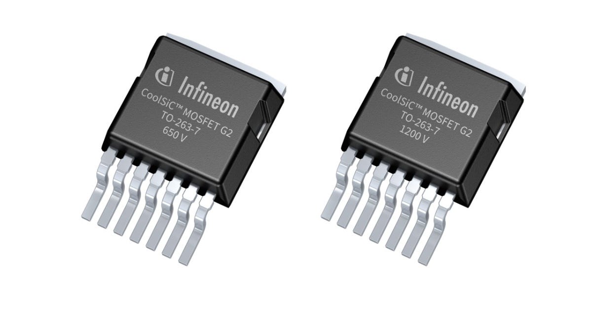
1200V SiC MOSFET (Infineon) for reduced part count in fast DC EV charging (Eliminated 4 switches in the topology) →
The absolute cost of SiC devices is higher than the cost of Si devices because of intrinsic higher material costs.
SiC MOSFETs are still about 3 to 5 times more expensive than Si-IGBT modules according to prices on Digi-Key →
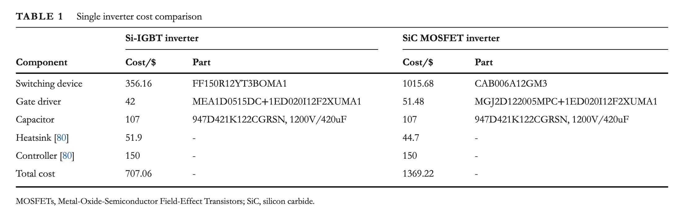
But the per-watt cost of the overall system could potentially be reduced with a better balance-of-plant system design.

The savings may come from developments such as a smaller passive component, lower cooling requirements, and a higher absolute power rating.Additionally, the operational cost reduction gained from efficiency improvements could justify the higher capital cost, e.g., in solar inverters (more yield) etc.
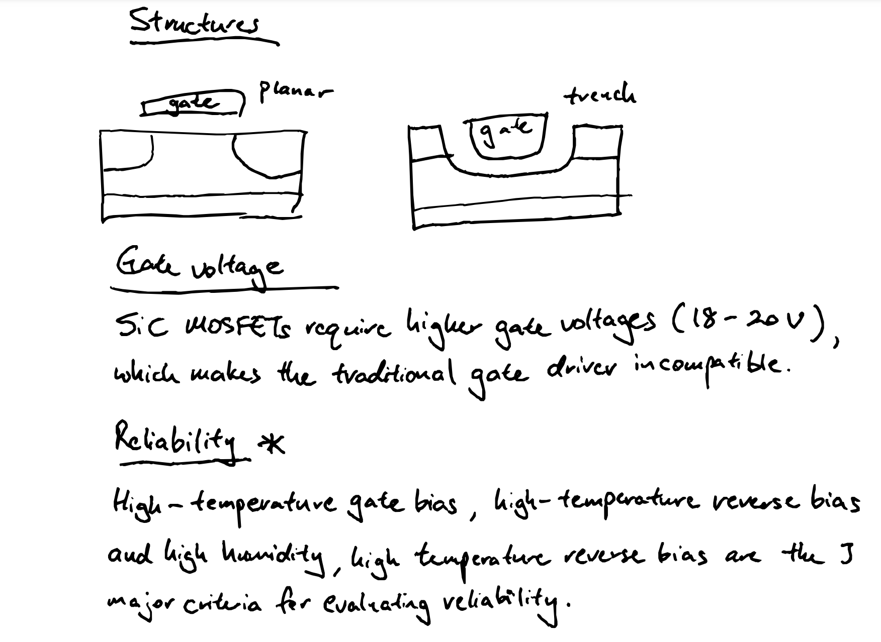
Comparing Si and SiC MOSFETs (Infineon)

Uncategorized scribbles


Notes
[1] SiC has many crystalline structures called polytypes that exhibit different physical properties because of periodic difference in the overlap of tetrahedrons. Common polytypes include 4H-SiC and 6H-SiC which are hexagonal crystal structures, and 3C-SiC which is a cubic crystal structure. 4H-SiC is commonly used because it provides a better balance among electron mobility, dielectric breakdown strength, saturation velocity, and other physical properties than other polytypes.
[2] SiC is also the only semiconductor other than Si that can oxidize thermally to for Si02 (which is an insulator). Which can make metal-oxide field effect transistors (MOSFETs).
Sources
Barbarini, Elena (June 25, 2018). STMicroelectronics SiC Module in Tesla Model3 Inverter
Toshiba Electronic Devices and Storage Corporation, 2020 Comparison of SiC MOSFET and Si IGBT
Xu She; Alex Q. Huang; Óscar Lucía; Burak Ozpineci Review of Silicon Carbide Power Devices and Their Applications
Bufan Shi, Anna Isabel Ramones, Yingxu Liu, Haoran Wang, Yu Li, Stefan Pischinger, Jakob Andert, A review of silicon carbide MOSFETs in electrified vehicles: Application, challenges, and future development
Evince Technology Limited, Why Diamond Is Better Than Anything Else
Kreutzer Otto, A passively cooled 15 kW, 800 V DCDC-converter with a peak efficiency of 99.7 %